


Easy
No MOQ, No high tooling cost, No high Starting fee Both Bulk or Full packaged components acceptable

Fast
Prototype PCB Assembled as fast as 24h Normal PCBA lead time 3-5wds

One-Stop
PCB Design+PCB manufacturing+PCB Assembly+Components Sourcing+Box Building
High-speed and high-precision PCBA production Lines
High-Speed: Yamaha placement machines, 300 thousand SMT points per hour; 2 shift to meet your quick lead time request
High-Precision: 0201 and 01005,0.25mm BGA,fine Pitch components as small as 0.3mm pitch.
Quickest only 8h for prototype PCB boards SMT Assembly

IQC Warehouse

SMD Stencll

Production Line 1& 2

Solderpaste Printing Machine

YAMAHA Pick and Place Machine

JUKl Pick and Place Machine

Reflow Oven

Wave-soldering
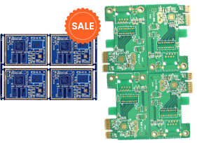
Limited Time Special Offer

PCB prototype
Volume production
PCB assembly(SMT+DIP)
Components sourcing worldwide
Hot Products
Double-layer board
Length and width within 10cm*5 pieces
Product Description:
- FR-4 TG150,1.6mm
- Normal delivery time 1-2 days
- National shipping
- 12/24 hours rush shipping available

Other Products
Four-layer
board
- ·FR-4 TG150, 1.6mm
- ·Normal delivery time 1-2 days

Six-layer
board
- ·FR-4 TG150, 1.6mm
- ·Normal delivery time 1-2 days

Single-sided
aluminum substrate
- ·FR-4 TG150, 1.6mm
- ·Normal delivery time 1-2 days


PCB Customization Services
Four-layer
board
- ·FR-4 TG150, 1.6mm
- ·Normal delivery time 1-2 days
Six-layer
board
- ·FR-4 TG150, 1.6mm
- ·Normal delivery time 1-2 days
Single-sided
aluminum substrate
- ·FR-4 TG150, 1.6mm
- ·Normal delivery time 1-2 days


Our PCB SMT Assembly Capability and Capacity

Full SMT PCB Assembly Service
- • Single and double-sided SMT Assembly
- • Full SMT PCB Assembly line
- • Low to high volume production assembly

PCB Types
- • Rigid board, Flexible board
- • Rigid-Flex Board, Aluminum PCB

Various Components Packages Available
- • BGA • QFN • SOIC
- • PLCC •QFP • UBGA
- • POP

High SMT Assembly Precision
- • Ultra Fine Pitch component: 0.25mm pitch
- • Smallest Component: 01005, 0201, 0402
- • Minimum BGA: 0.25mm pitch for rigid board
- • 0.4mm pitch for flex board
- • Assembly Accuracy: +/-0.025mm

Full Testing Services
- • Automated Optical Inspection
- • X-ray Testing
- • In-circuit Testing
- • Functional Testing

Capacity and Lead-Time
- • 6 Independent Assembly Lines
- • 300 thousand SMT points per hour
- • Only 8h for quick-turn prototype SMT Assembly order
Strict Quality Control
ISO9001, IATF16949, UL, Rohs Certificated
Strict production process control and Complete PCBA testing

lQC incoming Materialinspection

First Article Inspection

AOl inspection(after reflow soldering)

IPQC Full Line Inspection

X-RAY inspection Machine Detects BGA

QC Functional Test

QA Full Inspection
lQC incoming Materialinspection
First Article Inspection
AOl inspection(after reflow soldering)
IPQC Full Line Inspection
X-RAY inspection Machine Detects BGA
QC Functional Test
QA Full Inspection
Step 01
BGA is a common chip packaging technology whose dense array of solder balls is challenging for traditional visual inspection. X-ray inspection machines are able to penetrate the PCB surface and inspect the solder joints underneath the BGA. This non-invasive detection method can quickly and accurately detect welding defects, such as weak soldering, poor connections, etc., ensuring product quality and reliability.
Step 02
BGA is a common chip packaging technology whose dense array of solder balls is challenging for traditional visual inspection. X-ray inspection machines are able to penetrate the PCB surface and inspect the solder joints underneath the BGA. This non-invasive detection method can quickly and accurately detect welding defects, such as weak soldering, poor connections, etc., ensuring product quality and reliability.
Step 03
BGA is a common chip packaging technology whose dense array of solder balls is challenging for traditional visual inspection. X-ray inspection machines are able to penetrate the PCB surface and inspect the solder joints underneath the BGA. This non-invasive detection method can quickly and accurately detect welding defects, such as weak soldering, poor connections, etc., ensuring product quality and reliability.
Step 07
BGA is a common chip packaging technology whose dense array of solder balls is challenging for traditional visual inspection. X-ray inspection machines are able to penetrate the PCB surface and inspect the solder joints underneath the BGA. This non-invasive detection method can quickly and accurately detect welding defects, such as weak soldering, poor connections, etc., ensuring product quality and reliability.
Step 04
BGA is a common chip packaging technology whose dense array of solder balls is challenging for traditional visual inspection. X-ray inspection machines are able to penetrate the PCB surface and inspect the solder joints underneath the BGA. This non-invasive detection method can quickly and accurately detect welding defects, such as weak soldering, poor connections, etc., ensuring product quality and reliability.
Step 05
BGA is a common chip packaging technology whose dense array of solder balls is challenging for traditional visual inspection. X-ray inspection machines are able to penetrate the PCB surface and inspect the solder joints underneath the BGA. This non-invasive detection method can quickly and accurately detect welding defects, such as weak soldering, poor connections, etc., ensuring product quality and reliability.
Step 06
BGA is a common chip packaging technology whose dense array of solder balls is challenging for traditional visual inspection. X-ray inspection machines are able to penetrate the PCB surface and inspect the solder joints underneath the BGA. This non-invasive detection method can quickly and accurately detect welding defects, such as weak soldering, poor connections, etc., ensuring product quality and reliability.
Customer Reviews


Our expertise is here to serve you
How long have you been making PCB&PCBA?

PCBA make has been making PCBs for more than 26 years. We built our assembly plant and begin assembly business in 1996.
How do l get a quick quote for PCB or PCB assembly?
Please send your files and requirements to Orders@pcbamake.com. Quote will be sent back as soon as we get through an evaluation.
Do you cater SMT prototype boards?
Yes, we are fully equipped to handle your any kind of custom SMT prototype board requlrements. MOQ Is 1PCS.
What files and documents do you request for my PCBA orders?
Gerber Files/Bill of Materials, complete information in excel format Centroid Data/Other requirements or assembly instructions if applicable.
