

Quick Turn HDI PCB Manufacturer

HDI can't expedited? No, JH PCBA can expedite too!
6L,1 step HDI PCB,prototype,fastest 48h
10L,2-step HDI PCB,10 m2, fastest 10 days
8L,any layer connection HDI PCB, prototype, fastest 6 days
For new customers to try our quick manufacturing service, Free expedite fee or 50% deduction!
Quick-Turn HDI PCB We Manufacture

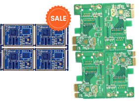
Data Acquisition Motherboard

Data Acquisition Motherboard

Data Acquisition Motherboard

Data Acquisition Motherboard

Data Acquisition Motherboard

Data Acquisition Motherboard

Data Acquisition Motherboard

Data Acquisition Motherboard
Data Acquisition Motherboard
Data Acquisition Motherboard
Data Acquisition Motherboard
Data Acquisition Motherboard
Data Acquisition Motherboard
Data Acquisition Motherboard
Data Acquisition Motherboard
Data Acquisition Motherboard

Affordable Prototype PcB Manufacturer in China
-
2019-08-08
 alexia 1320*10cm1-2 days
 -
2019-08-23alexia 1420*10cm1-2 days
-
2020-01-01alexia 1220*10cm1-2 days
-
2021-05-05alexia 1520*10cm1-2 days
-
2021-08-20alexia 1620*10cm1-2 days
-
2021-07-16alexia 1520*10cm1-2 days
-
2024-08-08alexia 1620*10cm1-2 days
-
2024-08-23alexia 1520*10cm1-2 days
-
2024-08-02alexia 1520*10cm1-2 days
-
2024-08-04alexia 1620*10cm1-2 days

753+
Last 30 days

5000+
Customers

99.8%
on time delivery
Quick-Turn PCB Prototype Orders
HDI PCB Structures We Support
| HDI PCB Structures | Microvia Categories | High-Volume Production | Small To Medium-Volume Production | Prototype | Availability |
|---|---|---|---|---|---|
| 1+N+1 | Blind vias | Yes | Yes | Yes | Over 4 layers |
| 2+N+2 | Blind/buried staggered vias | Yes | Yes | Yes | Over 6 layers |
| 2+N+2 | Blind/buried stacked vias | Yes | Yes | Yes | Over 6 layers |
| 3+N+3 | Blind/buried stacked vias | / | Yes | Yes | Over 8 layers |
| 3+N+3 | Blind/buried stacked vias | / | / | Yes | Over 8 layers |
HDI PCB Production Capacity
| Serial No | Item | Technical Parameters |
|---|---|---|
| 1 | Base Material | FR-4 | High Tg | Halogen-free | PTFE | Ceramic PCB | Polyimide |
| 2 | Board Type | PCB | FPC | R-FPC | HDI |
| 3 | Hignest Layer | 64Layer |
| 4 | Minimum base copper thickness | 1/3 OZ ( 12um ) |
| 5 | Maximum finished copper thickness | 8 OZ |
| 6 | Minimum trace / gap (Inner layer) | 2/2mil (H/H OZ base copper) |
| 7 | Maximum produce size | 609*889mm |
| 8 | Minimum trace / gap (Outer layer) | 2/2mil (1/3 OZ base copper) |
| 9 | Minimum distance from hole to inner conductor | 6mil |
| 10 | Minimum distance from hole to outer conductor | 6mil |
